(China (Mainland))

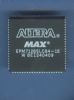
Product Summary
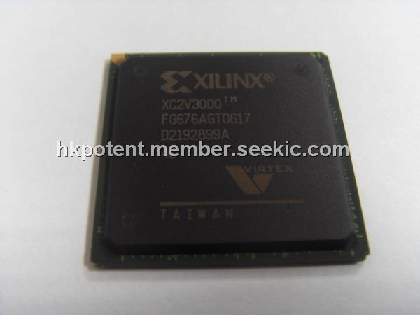
The XC2V3000FG676AGT is a platform FPGA developed for high performance from low-density to high-density designs that are based on IP cores and customized modules. The XC2V3000FG676AGT delivers complete solutions for telecommunication, wireless, networking, video, and DSP applications, including PCI, LVDS, and DDR interfaces. The XC2V3000FG676AGT leading-edge 0.15 μm / 0.12 μm CMOS 8-layer metal process and the Virtex-II architecture are optimized for high speed with low power consumption. Combining a wide variety of flexible features and a large range of densities up to 10 million system gates, the XC2V3000FG676AGT enhances programmable logic design capabilities and is a powerful alternative to mask-programmed gates arrays. The XC2V3000FG676AGT comprises 11 members, ranging from 40K to 8M system gates.
Parametrics
XC2V3000FG676AGT absolute maximum ratings: (1)VCCINT, Internal supply voltage relative to GND: –0.5 to 1.65 V; (2)VCCAUX, Auxiliary supply voltage relative to GND: –0.5 to 4.0 V; (3)VCCO, Output drivers supply voltage relative to GND: –0.5 to 4.0 V; (4)VBATT, Key memory battery backup supply: –0.5 to 4.0 V; (5)VREF, Input reference voltage: –0.5 to VCCO + 0.5 V; (6)VIN, Input voltage relative to GND (user and dedicated I/Os): –0.5 to VCCO + 0.5 V; (7)VTS, Voltage applied to 3-state output (user and dedicated I/Os): –0.5 to 4.0 V; (8)TSTG, Storage temperature (ambient): –65 to +150℃.
Features
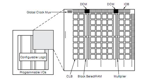
XC2V3000FG676AGT features: (1)Up to 93,184 internal registers / latches with Clock Enable; (2)Up to 93,184 look-up tables (LUTs) or cascadable 16-bit shift registers; (3)Wide multiplexers and wide-input function support; (4)Horizontal cascade chain and Sum-of-Products support; (5)Internal 3-state bussing; (6)Fast SelectMAP configuration; (7)Triple Data Encryption Standard (DES) security option (Bitstream Encryption); (8)IEEE1532 support; (9)Partial reconfiguration; (10)Unlimited re-programmability; (11)Readback capability; (12)Up to 1,108 user I/Os; (13)19 single-ended standards and six differential standards; (14)Programmable sink current (2 mA to 24 mA) per I/O; (15)Densities from 40K to 8M system gates; (16)420 MHz internal clock speed (Advance Data); (17)840+ Mb/s I/O (Advance Data).
Diagrams
 |
 XC2V1000 |
Other |
|
Data Sheet |
Negotiable |
|
||||||
|
XC2V1000-4BG575I |
|
IC FPGA VIRTEX-II 575PBGA |
Data Sheet |
|
|
||||||
 |
XC2V1000-4BGG575C |
|
IC VIRTEX-II FPGA 1M 575-MBGA |
Data Sheet |
|
|
||||||
|
XC2V1000-4BGG575I |
|
IC FPGA VIRTEX-II 2M 575-MBGA |
Data Sheet |
|
|
||||||
|
XC2V1000-4FF896I |
|
IC FPGA VIRTEX-II 896FCBGA |
Data Sheet |
|
|
||||||
|
XC2V1000-4FFG896C |
|
IC VIRTEX-II FPGA 1M 896-FBGA |
Data Sheet |
|
|
||||||