(China (Mainland))

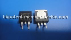
Product Summary
The STB25NM50N is a revolutionary MOSFET. The STB25NM50N is realized with the second generation of MDmesh Technology. It associates a new vertical structure to the Company’s strip layout to yield one of the world’s lowest on-resistance and gate charge. It is therefore suitable for the most demanding high efficiency converters. TheSTB25NM50N is very suitable for increasing power density of high voltage converters allowing system miniaturization and higher efficiencies.
Parametrics
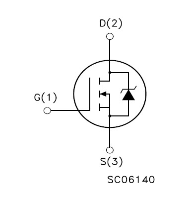
STB25NM50N absolute maximum ratings: (1)VDS Drain-source Voltage (VGS = 0): 500V; (2)VDGR Drain-gate Voltage (RGS = 20kΩ): 500V; (3)VGS Gate- source Voltage: ±25V; (4)ID Drain Current (continuous) at TC = 25℃: 22A; (5)ID Drain Current (continuous) at TC = 100℃: 14A; (6)IDM Drain Current (pulsed): 88A; (7)PTOT Total Dissipation at TC = 25℃: 160W; (8)Derating Factor: 1.28W/℃; (9)dv/dt Peak Diode Recovery voltage slope: 15V/ns; (10)Tstg Storage Temperature: -55℃ to 150℃; (11)Tj Max. Operating Junction Temperature: 150℃.
Features
STB25NM50N features: (1) high dv/dt and avalanche capabilities; (2)100% avalanche tested; (3) low input capacitance and gate charge; (4) low gate input resistance.
Diagrams
| Image | Part No | Mfg | Description |  |
Pricing (USD) |
Quantity | ||||
|---|---|---|---|---|---|---|---|---|---|---|
 |
 STB25NM50N |
STMicroelectronics |
MOSFET N Ch 550V TJMAX 0.12 Ohm 21.5A |
Data Sheet |
Negotiable |
|
||||
|
STB25NM50N-1 |
STMicroelectronics |
MOSFET N-CHANNEL MFT |
Data Sheet |
Negotiable |
|
||||