(China (Mainland))

Product Summary
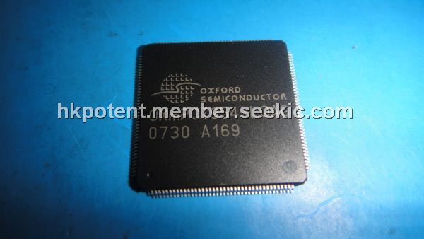
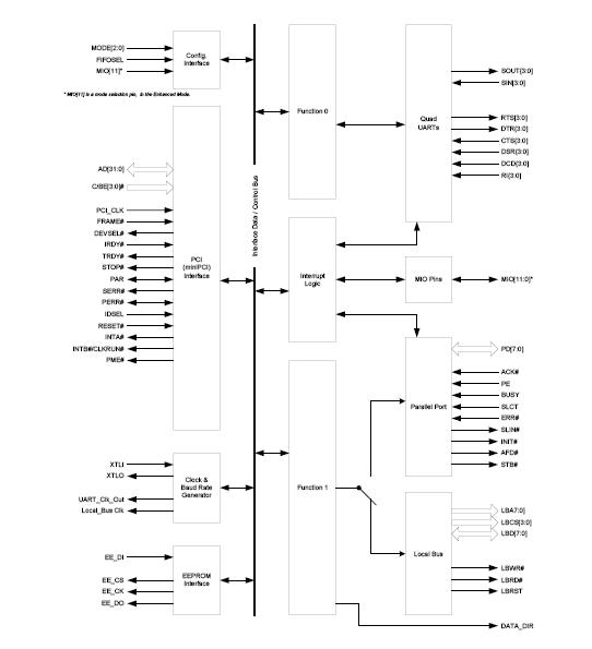
The OXMPCI954-LQAG is a single chip solution for PCI and mini- PCI based serial and parallel expansion add-in cards. It is a dual function PCI device, where function 0 offers four ultra-high performance OX16C950 UARTs, and function 1 is configurable either as an 8-bit Local Bus or a bidirectional parallel port. Each UART channel in the OXMPCI954-LQAG is the fastest available PC-compatible UART, offering data rates up to 15Mbps and 128-byte deep transmitter and receiver FIFOs. The deep FIFOs reduce CPU overhead and allow utilisation of higher data rates. Each UART channel is software compatible with the widely used industry-standard 16C550 devices (and compatibles). In addition to increased performance and FIFO size, the UARTs also provide the full set of OXMPCI954-LQAG enhanced features including automated in-band flow control, readable FIFO levels etc.
Parametrics
OXMPCI954-LQAG absolute maximum ratings: (1)VDD DC supply voltage: -0.3V to 3.8V; (2)VIN DC input voltage: -0.3V to VDD + 0.3V; (3)VIN_5V DC input voltage: – 5V tolerant -0.3V to 5.6V; (4)IIN DC input current: ±10mA; (5)TSTG Storage temperature: -40℃ to 125℃.
Features
OXMPCI954-LQAG features: (1)Software compatible with OX16PCI954; (2)Four 16C950 High performance UART channels; (3)8-bit Pass-through Local Bus (PCI Bridge); (4)IEEE1284 Compliant SPP/EPP/ECP parallel port (with external transceiver); (5)Efficient 32-bit, 33MHz, Multi-function target-only PCI controller, fully compliant to PCI Local Bus specification 3.0, and PCI Power Management Specification 1.1; (6)PCI and miniPCI Modes (with CLKRUN# and D3cold support in miniPCI modes); (7)UARTs fully software compatible with 16C550-type devices.; (8)UART operation up to 60 MHz via external clock source. Up to 20MHz with the crystal oscillator.; (9)Baud rates up to 60Mbps in external 1x clock mode and 15Mbps in asynchronous mode.; (10)128-byte deep FIFO per transmitter and receiver; (11)Flexible clock prescaler, from 1 to 31.875; (12)Automated in-band flow control using programmable Xon/Xoff in both directions; (13)Automated out-of-band flow control using CTS#/RTS# and/or DSR#/DTR#; (14)Arbitrary trigger levels for receiver and transmitter FIFO interrupts and automatic in-band and out-of-band flow control; (15)Infra-red (IrDA) receiver and transmitter operation; (16)9-bit data framing, as well as 5,6,7 and 8 bits; (17)Detection of bad data in the receiver FIFO; (18)Global Interrupt Status and readable FIFO levels to facilitate implementation of efficient device drivers; (19)Local registers to provide status/control of device functions.; (20)12 multi-purpose I/O pins, which can be configured as input interrupt pins or wake-up; (21)Auto-detection of a wide range of optional MicrowireTM compatible EEPROMs, to re-configure device parameters; (22)Function access, to pre-configure each function prior to handover to generic device drivers; (23)Operation via IO or memory mapping; (24)3.3V operation (5v tolerance on selected I/Os); (25)Extended Operating Temp. Range : -40℃ to 105℃; (26)160-pin LQFP or 176-pin VBGA package.
Diagrams
 |
 OXmPCI952 |
Other |
|
Data Sheet |
Negotiable |
|
||||
|
OXmPCI954 |
Other |
|
Data Sheet |
Negotiable |
|
||||