(China (Mainland))

Product Summary
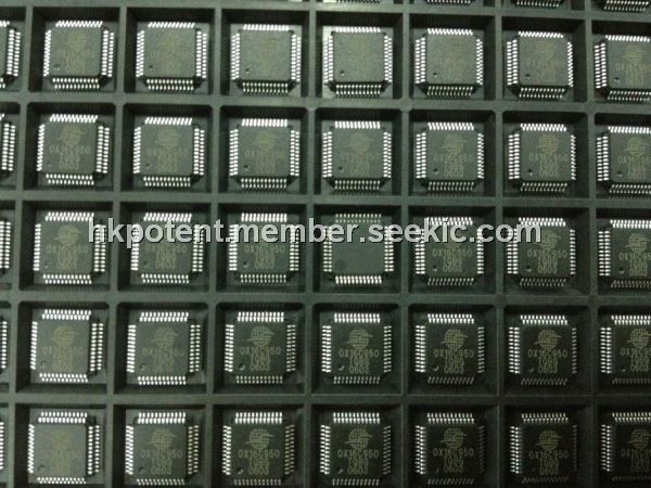
The OX16C950-TQBG is a single-channel ultra-high performance UART offering data rates up to 15Mbps and 128-deep transmitter and receiver FIFOs. Deep FIFOs reduce CPU overhead and allow utilisation of higher data rates. It is software compatible with the widely used industry standard 16C550 type devices and compatibles, as well as other OX16C95x family devices. The OX16C950-TQBG is pin-compatible with the TL16C550, ST16C650 devices. In addition to increased performance and FIFO size, the OX16C950-TQBG also provides enhanced features including improved flow control. Automated software flow control using Xon/Xoff and automated hardware flow control using CTS#/RTS# and DSR#/DTR# prevent FIFO over-run. Flow control and interrupt thresholds are fully programmable and readable, enabling programmers to fine-tune the performance of their system. FIFO levels are readable to facilitate fast driver applications.
Parametrics
OX16C950-TQBG absolute maximum ratings: (1)VDD DC supply voltage: -0.3 to 7.0V; (2)VIN DC input voltage: -0.3 to VDD + 0.3V; (3)IIN DC input current: ±10mA; (4)TSTG Storage temperature: -40 to 125℃.
Features
OX16C950-TQBG features: (1)Single full-duplex asynchronous channel; (2)128-byte deep transmitter / receiver FIFO; (3)Fully software compatible with industry standard 16C550 type UARTs; (4)Pin compatible with TL16C550B/C, ST16C650 and TL16C750; (5)IBM PC/AT compatible; (6)Baud rates up to 15 Mbps in normal mode and 60Mbps in external 1x clock mode; (7)Readable FIFO levels; (8)Flexible clock prescaler from 1 to 31.875; (9)Isochronous mode using external 1x baud rate clock up to 60Mbps; (10)9-bit data framing as well as 5,6,7 and 8; (11)Detection of bad data in the receiver FIFO; (12)Automated in-band flow control using programmable Xon/Xoff characters; (13)Transmitter and receiver can be disabled; (14)Automated out-of-band flow control using CTS# / RTS# and DSR# / DTR#; (15)Readable in-band and out-of-band flow control status; (16)Programmable special character detection; (17)Arbitrary trigger levels for receiver and transmitter FIFO interrupts and automatic in-band and out-of-band flow control; (18)Transmitter idle interrupt (shift register and FIFO both empty); (19)Optional Infra-red (IrDA) receiver and transmitter operation; (20)RS-485 buffer enable signals; (21)Software channel reset; (22)Four byte device ID; (23)Sleep mode (low operating current); (24)System clock up to 60 MHz (at 5V), 50 MHz at 3.3V; (25)44 PLCC and 48 TQFP packages; (26)5 volts operation (PLCC), 3.3/ 5V operation TQFP.
Diagrams

| Image | Part No | Mfg | Description |  |
Pricing (USD) |
Quantity | ||||||||||
|---|---|---|---|---|---|---|---|---|---|---|---|---|---|---|---|---|
 |
 OX16C950-TQBG |
PLX Technology |
Peripheral Drivers & Components (PCIs) High performance single UART |
Data Sheet |
|
|
||||||||||
| Image | Part No | Mfg | Description | |
Pricing (USD) |
Quantity | ||||||||||
|
OX16C950 |
Other |
|
Data Sheet |
Negotiable |
|
||||||||||
|
OX16C950B |
Other |
|
Data Sheet |
Negotiable |
|
||||||||||
|
OX16C950-TQBG |
PLX Technology |
Peripheral Drivers & Components (PCIs) High performance single UART |
Data Sheet |
|
|
||||||||||
|
OX16C954 |
Other |
|
Data Sheet |
Negotiable |
|
||||||||||
|
OX16C954B |
Other |
|
Data Sheet |
Negotiable |
|
||||||||||
|
OX16C954-TQBG |
PLX Technology |
Peripheral Drivers & Components (PCIs) High performance quad UART |
Data Sheet |
|
|
||||||||||