(China (Mainland))

Product Summary
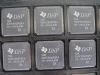
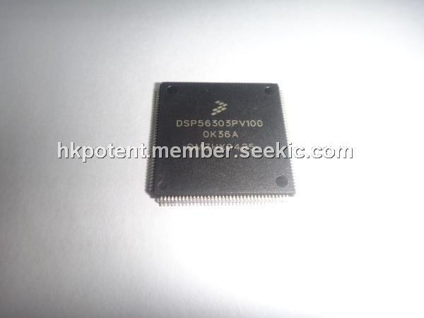
The DSP56303PV100 is a 24-Bit, Digital Signal Processor. The features of it include a barrel shifter, 24-bit addressing, instruction cache, and DMA. The DSP56303PV100 offers 100 MMACS using an internal 100 MHz clock at 3.0–3.6 volts. The DSP56303PV100 offers a rich instruction set and low power dissipation, as well as increasing levels of speed and power to enable wireless, telecommunications, and multimedia products.
Parametrics
DSP56303PV100 absolute maximum ratings: (1)Supply Voltage VCC: -0.3 to +4.0 V; (2)All input voltages excluding 5 V tolerant inputs VIN: GND -0.3 to VCC + 0.3 V; (3)All 5 V tolerant input voltages VIN5: GND -0.3 to 5.5 V; (4)Current drain per pin excluding VCC and GND, I: 10 mA; (5)Operating temperature range TJ: -40 to +100 ℃; (6)Storage temperature TSTG: -55 to +150 ℃.
Features
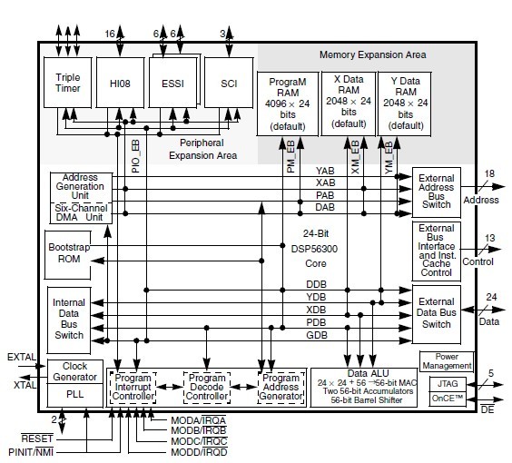
DSP56303PV100 features: (1)100 million multiply-accumulates per second (MMACS) with a 100 MHz clock at 3.3 V nominal; (2)Object code compatible with the DSP56000 core with highly parallel instruction set; (3)Data arithmetic logic unit (Data ALU) with fully pipelined 24*24-bit parallel multiplier-accumulator (MAC), 56-bit parallel barrel shifter (fast shift and normalization; bit stream generation and parsing), conditional ALU instructions, and 24-bit or 16-bit arithmetic support under software control; (4)Phase-lock loop (PLL) allows change of low-power divide factor (DF) without loss of lock and output clock with skew elimination; (5)Hardware debugging support including on-chip emulation (OnCE module, Joint Test Action Group (JTAG) test access port (TAP); (6)192x24-bit bootstrap ROM; (7)8 Kx24-bit RAM total; (8)Program RAM, instruction cache, X data RAM, and Y data RAM sizes are programmable; (9)External memory expansion port; (10)Chip select logic for glueless interface to static random access memory (SRAMs); (11)Internal DRAM Controller for glueless interface to dynamic random access memory (DRAMs); (12)Very low-power CMOS design; (13)Wait and Stop low-power standby modes; (14)Fully static design specified to operate down to 0 Hz (dc); (15)Optimized power management circuitry (instruction-dependent, peripheral-dependent, and mode-dependent).
Diagrams
 |
 DSP56001 |
Other |
|
Data Sheet |
Negotiable |
|
||||
|
DSP56001A |
Other |
|
Data Sheet |
Negotiable |
|
||||
|
DSP56002 |
Other |
|
Data Sheet |
Negotiable |
|
||||
|
DSP56004 |
Other |
|
Data Sheet |
Negotiable |
|
||||
|
DSP56005 |
Other |
|
Data Sheet |
Negotiable |
|
||||
|
DSP56007 |
Other |
|
Data Sheet |
Negotiable |
|
||||