(China (Mainland))


Product Summary
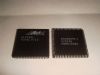
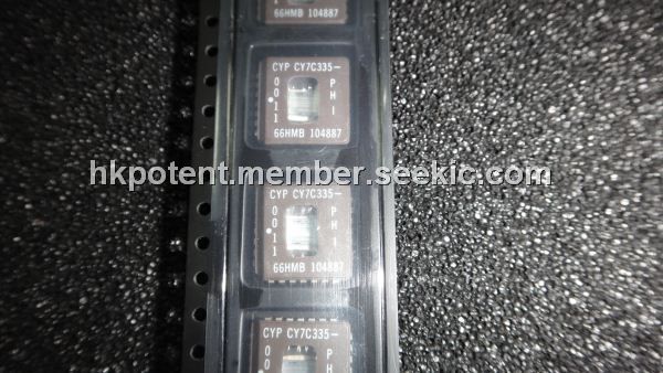
The CY7C335-66HMB is a Universal Synchronous EPLD whose architecture has been optimized to enable the user to easily and efficiently construct very high performance state machines. The architecture of the CY7C335-66HMB, consisting of the user-configurable output macrocell, bidirectional I/O capability, input registers, and three separate clocks, enables the user to design high-performance state machines that can communicate either with each other or with microprocessors over bidirectional parallel buses of user-definable widths. The four clocks of the CY7C335-66HMB permit independent, synchronous state machines to be synchronized to each other.
Parametrics
CY7C335-66HMB absolute maximum ratings: (1)Storage Temperature:–65℃ to +150℃; (2)Ambient Temperature with Power Applied: –55℃ to +125℃; (3)Supply Voltage to Ground Potential (Pin 22 to Pins 8 and 21):–0.5V to +7.0V; (4)DC Voltage Applied to Outputs; (5)in High Z State:–0.5V to +7.0V; (6)DC Input Voltage:–3.0V to +7.0V; (7)Output Current into Outputs (Low): 12mA; (8)Static Discharge Voltage: >2001V (per MIL-STD-883, Method 3015); (9)Latch-Up Current: >200mA; (10)DC Programming Voltage: 13.0V.
Features
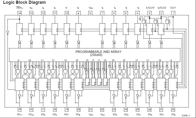
CY7C335-66HMB features: (1)100-MHz output registered operation; (2)Twelve I/O macrocells, each having; (3)Registered, three-state I/O pins; (4)Input and output register clock select multiplexer; (5)Feed back multiplexer; (6)Output enable (OE) multiplexer; (7)Bypass on input and output registers; (8)All twelve macrocell state registers can be hidden; (9)User configurable I/O macrocells to implement JK or RS flip-flops and T or D registers; (10)Input multiplexer per pair of I/O macrocells allows I/O pin associated with a hidden macrocell state register to be saved for use as an input; (11)Four dedicated hidden registers; (12)Twelve dedicated registered inputs with individually programmable bypass option; (13)Three separate clocks-two input clocks, two output clocks; (14)Common (pin 14-controlled) or product term-controlled output enable for each I/O pin; (15)256 product terms?2 per pair of macrocells, variable distribution; (16)Global, synchronous, product term-controlled, state register set and reset-inputs to product term are clocked by input clock; (17)2-ns input set-up and 9-ns output register clock to output; (18)0-ns input register clock to state register clock; (19)28-pin, 300-mil DIP, LCC, PLCC; (20)Erasable and reprogrammable; (21)Programmable security bit.
Diagrams
 |
 CY7C006 |
Other |
|
Data Sheet |
Negotiable |
|
||||||||||||
|
CY7C006A |
Other |
|
Data Sheet |
Negotiable |
|
||||||||||||
 |
CY7C006A-15AXC |
Cypress Semiconductor |
SRAM 5V 16Kx8 COM Dual Port SRAM |
Data Sheet |
Negotiable |
|
||||||||||||
|
CY7C006A-15AXCT |
Cypress Semiconductor |
SRAM 5V 16Kx8 COM Dual Port SRAM |
Data Sheet |
Negotiable |
|
||||||||||||
 |
CY7C006A-20AC |
|
IC SRAM 16KX8 DUAL 64LQFP |
Data Sheet |
Negotiable |
|
||||||||||||
|
CY7C006A-20AXC |
Cypress Semiconductor |
SRAM 5V 16Kx8 COM Dual Port SRAM |
Data Sheet |
|
|
||||||||||||