(China (Mainland))

Product Summary
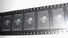
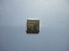
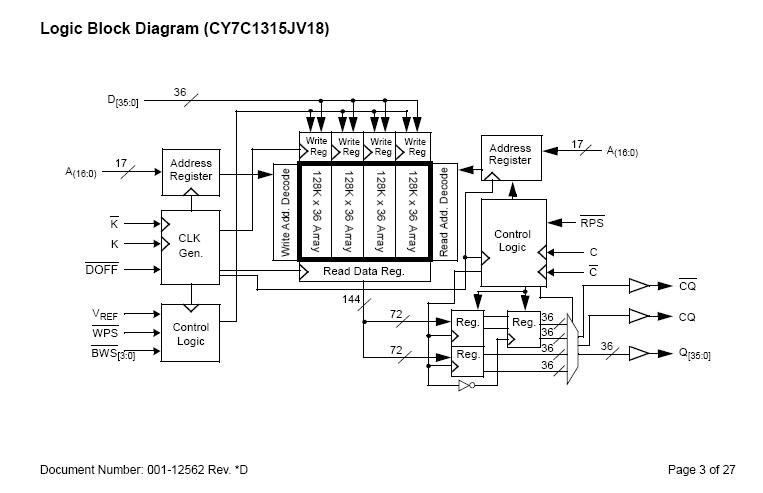
The CY7C1315JV18-300BZC is a 1.8V Synchronous Pipelined SRAM, equipped with QDR II architecture. QDR II architecture consists of two separate ports: the read port and the write port to access the memory array. The read port has dedicated data outputs to support read operations and the write port has dedicated data inputs to support write operations. QDR II architecture has separate data inputs and data outputs to eliminate the need to ‘turnaround’ the data bus required with common IO devices. Access to each port is accomplished through a common address bus. Addresses for read and write addresses are latched on alternate rising edges of the input (K) clock. Accesses to the QDR II read and write ports are completely independent of one another. In order to maximize data throughput, both read and write ports are provided with DDR interfaces. Each address location is associated with four 36-bit words that burst sequentially into or out of the CY7C1315JV18-300BZC. Because data is transferred into and out of the CY7C1315JV18-300BZC on every rising edge of both input clocks (K and K and C and C), memory bandwidth is maximized while simplifying system design by eliminating bus ‘turnarounds’.
Parametrics
CY7C1315JV18-300BZC absolute maximum ratings: (1)Storage Temperature:–65℃ to +150℃; (2)Ambient Temperature with Power Applied:–55℃ to +125℃; (3)Supply Voltage on VDD Relative to GND:–0.5V to +2.9V; (4)Supply Voltage on VDDQ Relative to GND:–0.5V to +VDD; (5)DC Applied to Outputs in High-Z:–0.5V to VDDQ + 0.3V; (6)DC Input Voltage:–0.5V to VDD + 0.3V; (7)Current into Outputs (LOW): 20mA; (8)Static Discharge Voltage (MIL-STD-883, M. 3015): >2001V; (9)Latch-up Current: >200mA.
Features
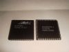
CY7C1315JV18-300BZC features: (1)Separate Independent Read and Write Data Ports; (2)Supports concurrent transactions; (3)300 MHz Clock for High Bandwidth; (4)4-word Burst for reducing Address Bus Frequency; (5)Double Data Rate (DDR) interfaces on both read and write ports; (6)(data transferred at 600 MHz) at 300 MHz; (7)Two Input Clocks (K and K) for Precise DDR Timing; (8)SRAM uses rising edges only; (9)Two Input Clocks for Output Data (C and C) to minimize Clock Skew and Flight Time mismatches; (10)Echo Clocks (CQ and CQ) simplify Data Capture in High Speed Systems; (11)Single Multiplexed Address Input Bus latches Address Inputs for both Read and Write Ports; (12)Separate Port Selects for Depth Expansion; (13)Synchronous Internally Self-timed Writes; (14)QDR. II Operates with 1.5 Cycle Read Latency when the Delay Lock Loop (DLL) is enabled; (15)Operates like a QDR I device with 1 Cycle Read Latency in DLL Off Mode; (16)Available in x8, x9, x18, and x36 configurations; (17)Full Data Coherency, providing most current Data; (18)Core VDD = 1.8 (±0.1V); IO VDDQ = 1.4V to VDD; (19)Available in 165-Ball FBGA Package (13 x 15 x 1.4 mm); (20)Offered in both Pb-free and non Pb-free packages; (21)Variable Drive HSTL Output Buffers; (22)JTAG 1149.1 Compatible Test Access Port; (23)Delay Lock Loop (DLL) for Accurate Data Placement.
Diagrams
| Image | Part No | Mfg | Description |  |
Pricing (USD) |
Quantity | ||||||||||||
|---|---|---|---|---|---|---|---|---|---|---|---|---|---|---|---|---|---|---|
 |
 CY7C1315JV18-300BZC |
Cypress Semiconductor |
SRAM 512Kx36 1.8V QDR II (4-Word Burst) |
Data Sheet |
Negotiable |
|
||||||||||||
| Image | Part No | Mfg | Description | |
Pricing (USD) |
Quantity | ||||||||||||
|
CY7C006 |
Other |
|
Data Sheet |
Negotiable |
|
||||||||||||
|
CY7C006A |
Other |
|
Data Sheet |
Negotiable |
|
||||||||||||
 |
CY7C006A-15AXC |
Cypress Semiconductor |
SRAM 5V 16Kx8 COM Dual Port SRAM |
Data Sheet |
Negotiable |
|
||||||||||||
|
CY7C006A-15AXCT |
Cypress Semiconductor |
SRAM 5V 16Kx8 COM Dual Port SRAM |
Data Sheet |
Negotiable |
|
||||||||||||
 |
CY7C006A-20AC |
|
IC SRAM 16KX8 DUAL 64LQFP |
Data Sheet |
Negotiable |
|
||||||||||||
|
CY7C006A-20AXC |
Cypress Semiconductor |
SRAM 5V 16Kx8 COM Dual Port SRAM |
Data Sheet |
|
|
||||||||||||