(China (Mainland))

Product Summary
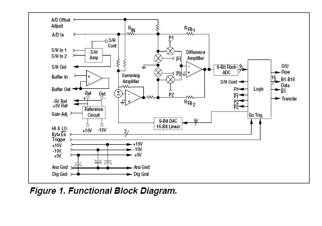
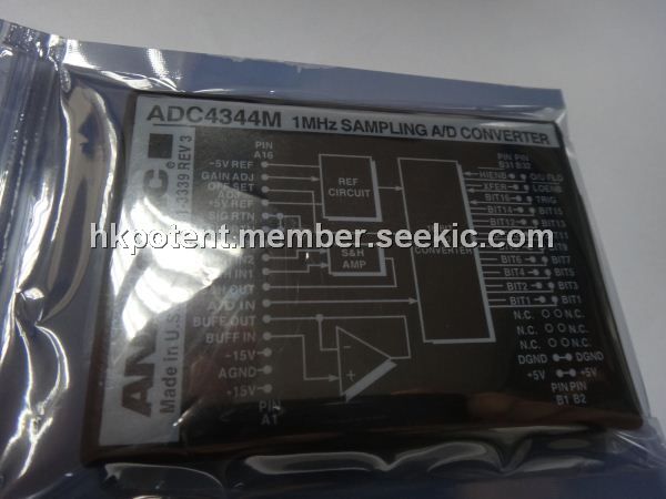
The ADC4344M is a complete 16-bit, 1 MHz and 500 kHz A/D converter subsystem with a built-in sample-and-hold amplifier in a space-saving 2.5" x 3.5" x 0.44" package. It offers pin-programmable input voltage ranges of ±2.5V, ±5V and 0 to +10V. It is designed for use in applications requiring high speed and high resolution front ends such as ATE, digital oscilloscopes, medical imaging, radar, sonar, and analytical instrumentation. The ADC4344M is capable of digitizing a 500 kHz signal at a 1 MHz sampling rate with a guarantee of no missing codes from 0℃ to +60℃. Equally impressive in frequency domain applications, the ADC4344M features 95 dB signal-to-noise ratio with input signals from DC to 100 kHz. The applications of the ADC4344M include Digital Signal Processing, Sampling Oscilloscopes, Automatic Test Equipment, High-Resolution Imaging, Analytical Instrumentation, Medical Instrumentation, CCD Detectors, IR Imaging, Sonar, and Radar.
Parametrics
ADC4344M absolute maximum ratings: (1)Voltage: ±5V, ±0.1% Max; (2)Stability: 10ppm/℃ Max.; (3)Available Current: 0.5mA Max.; (4)Input Bias Current: 10nA Max.; (5)Input Resistance: 100MΩ Typ.; (6)Input Capacitance: 10pF Typ.; (7)F.S. Settling Time: 800ns Typ. to 0.0015%.
Features
ADC4344M features: (1)Built-in S/H Amplifier; (2)Unique 2-Pass Sub-Ranging Architecture; (3)16-Bit Resolution; (4)1 MHz and 500 kHz Conversion Rate; (5)0.003% Maximum Integral Nonlinearity; (6)No Missing Codes; (7)Peak Distortion: –99dB (100 kHz Input); (8)Signal to Noise Ratio: 100 kHz; (9)Input 92 dB, ADC4344; 95dB, ADC4345; (10)Total Harmonic Distortion: –93dB (100kHz Input); (11)TTL/CMOS Compatibility; (12)Low Noise; (13)Compact Size: 2.5" x 3.5" x 0.44"; (14)Electromagnetic/Electrostatic Shielding.
Diagrams