(China (Mainland))

Product Summary
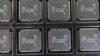
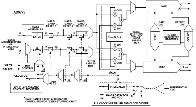
The AD9775BSV is a D/A converter. The AD9775BSV is the 14-bit pin-compatible, high performance, programmable 2×/4×/8× interpolating TxDAC+. The AD9775BSV features a serial port interface (SPI) providing a high level of programmability, thus allowing for enhanced system-level options. These options include: selectable 2×/4×/8× interpolation filters; fS/2, fS/4, or fS/8 digital quadrature modulation with image rejection; a direct IF mode; programmable channel gain and offset control; programmable internal clock divider; straight binary or two’s complement data interface; and a single-port or dual-port data interface. The applications of AD9775BSV include Communications, Analog Quadrature Modulation Architectures 3G, Multicarrier GSM, TDMA, CDMA systems broadband wireless, point-to-point microwave radios instrumentation/ATE.
Parametrics
AD9775BSV absolute maximum ratings: (1)AVDD, DVDD, CLKVDD, AGND, DGND, CLKGND: -0.3 to +4.0 V; (2)AVDD, DVDD, CLKVDD, AVDD, DVDD, CLKVDD: -4.0 to +4.0 V; (3)AGND, DGND, CLKGND, AGND, DGND, CLKGND: -0.3 to +0.3 V; (4)REFIO, REFLO, FSADJ1/2, AGND: -0.3 to AVDD + 0.3 V; (5)IOUTA, IOUTB, AGND: -1.0 to AVDD + 0.3 V; (6)P1B13–P1B0, P2B13–P2B0, DGND: -0.3 to DVDD + 0.3 V; (7)DATACLK, PLL_LOCK, DGND: -0.3 to DVDD + 0.3 V; (8)CLK+, CLK–, RESET, CLKGND: -0.3 to CLKVDD + 0.3 V; (9)LPF, CLKGND: -0.3 to CLKVDD + 0.3 V; (10)SPI_CSB, SPI_CLK, DGND: -0.3 to DVDD + 0.3 V; (11)SPI_SDIO, SPI_SDO Junction Temperature: -65 to +125℃; Storage Temperature: -65 to +150℃; Lead Temperature (10 sec): -65 to +300℃.
Features
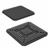
AD9775BSV features: (1)14-Bit Resolution, 160/400 MSPS Input/Output Data Rate; (2)Selectable 2×/4×/8× Interpolating Filter; (3)Programmable Channel Gain and Offset Adjustment; (4)fS/4, fS/8 Digital Quadrature Modulation Capability; (5)Direct IF Transmission Mode for 70 MHz + IFs; (6)Enables Image Rejection Architecture; (7)Fully Compatible SPI Port; (8)Excellent AC Performance, SFDR –71 dBc @ 2 MHz–35 MHz; WCDMA ACPR –71 dB @ IF = 71 MHz; (9)Internal PLL Clock Multiplier; (10)Selectable Internal Clock Divider; (11)Versatile Clock Input, Differential/Single-Ended Sine Wave or; TTL/CMOS/LVPECL Compatible; (12)Versatile Input Data Interface, Two’s Complement/Straight Binary Data Coding; Dual-Port or Single-Port Interleaved Input Data; (13)Single 3.3 V Supply Operation; (14)Power Dissipation: Typical 1.2 W @ 3.3 V; (15)On-Chip 1.2 V Reference; (16)80-Lead Thermally Enhanced TQFP Package.
Diagrams
| Image | Part No | Mfg | Description |  |
Pricing (USD) |
Quantity | ||||||||||||||
|---|---|---|---|---|---|---|---|---|---|---|---|---|---|---|---|---|---|---|---|---|
 |
 AD9775BSV |
Analog Devices Inc |
IC DAC 14BIT DUAL 160MSPS 80TQFP |
Data Sheet |
|
|
||||||||||||||
|
AD9775BSVRL |
Analog Devices Inc |
IC DAC 14BIT DUAL 160MSPS 80TQFP |
Data Sheet |
Negotiable |
|
||||||||||||||
 |
AD9775BSVZ |
|
IC DAC 14BIT DUAL 160MSPS 80TQFP |
Data Sheet |
|
|
||||||||||||||
|
AD9775BSVZRL |
|
IC DAC 14BIT DUAL 160MSPS 80TQFP |
Data Sheet |
|
|
||||||||||||||