(China (Mainland))


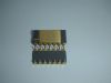
Product Summary
The MTW32N25E is an advanced Power MOSFET. The MTW32N25E is designed to withstand high energy in the avalanche and commutation modes. The new energy efficient design also offers a drain–to–source diode with a fast recovery time. Designed for low voltage, high speed switching applications in power supplies, converters and PWM motor controls, the MTW32N25E is particularly well suited for bridge circuits where diode speed and commutating safe operating areas are critical and offer additional safety margin against unexpected voltage transients.
Parametrics
MTW32N25E absolute maximum ratings: (1)Drain–Source Voltage VDSS: 250Vdc; (2)Drain–Gate Voltage (RGS = 1.0MΩ) VDGR: 250Vdc; (3)Gate–Source Voltage Continuous: ±20Vdc; (4)Non–Repetitive (tp 3 10 ms): ±40Vpk; (5)Drain Current-Continuous: 32Adc; (6)Drain Current-Continuous @ 100℃: 25Adc; (7)Drain Current-Single Pulse (tp ≤10μs): 96Apk; (8)Total Power Dissipation: 250W; (9)Derate above 25℃: 2.0W/℃; (10)Operating and Storage Temperature Range TJ, Tstg: –55 to 150℃; (11)Single Pulse Drain–to–Source Avalanche Energy – Starting TJ = 25℃ (VDD = 100Vdc, VGS = 10Vdc, IL = 20Apk, L = 3.0mH, RG = 25Ω) EAS: 600mJ; (12)Thermal Resistance–Junction to Case: 0.05℃/W; (13)Thermal Resistance–Junction to Ambient: 40℃/W; (14)Maximum Lead Temperature for Soldering Purposes, 1/8, from case for 10 sec TL: 260℃.
Features
MTW32N25E features: (1)Avalanche Energy Specified; (2)Source-to-Drain Diode Recovery Time Comparable to a Discrete Fast Recovery Diode; (3)Diode is Characterized for Use in Bridge Circuits; (4)IDSS and VDS(on) Specified at Elevated Temperature; (5)Isolated Mounting Hole Reduces Mounting Hardware.
Diagrams